Kyocera’s advanced ceramic plays a crucial role in microchip production
Kyocera’s silicon nitride acts as a carrier material for several tens of thousands of microscopic contact needles, which are used to check the functionality of chips during the production.
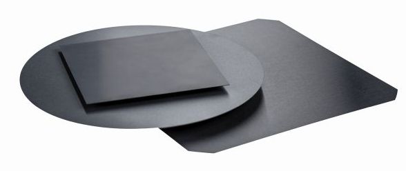
- Fine Ceramic Components
Kyoto/London − Microchips have become an indispensable part of everyday life: they can be found in countless objects such as smartphones, credit cards, cars and even medical devices. Kyocera’s high-end ceramic material Starceram N3000 P plays an important role in testing the functionality of microchips. Once processors and memory chips have been produced on a silicon wafer, a detailed test of the functionality of the electronic circuits follows. In the interest of efficiency, this test is conducted directly on the silicon wafer, after which only those chips that have been identified as functioning correctly are physically separated.
Ceramic carrier plate with several tens of thousands of microscopic contact needles
In order to check out the functional testing, so-called probe cards are used. This is a measuring head fitted with several tens of thousands of microscopic contact needles that are inserted into a very thin silicon nitride plate produced by Kyocera. The needles are put in contact with the chip surface. This is used to exchange signals with the test system, which in turn checks the functionality of the chip. The silicon nitride plate keeps the needles in the correct position to guarantee accurate measurements. At the same time, the contact needles must be able to spring back along their longitudinal axis to ensure that they touch down softly on the silicon surface. The silicon nitride must have excellent strength and high electrical resistance in order to ensure that the panel is stable and to avoid interference with the signal transmission.
Outstanding material properties to cater for a wide range of operating conditions
The guide holes for the contact needles are drilled into the material using a laser process. Constantly decreasing structure widths in microchip production in turn make it necessary to continue improving the precision in drilling these apertures. To achieve this, the silicon nitride plates must be designed to be even thinner. Kyocera offers material thicknesses of between 0.125 mm and in excess of 1 mm. The Starceram N3000 P advanced ceramic developed by Kyocera combines the necessary strength, low wear and the required ability to slide back and forth in the guide holes. The functionality of the microchips is tested for different operating conditions ranging from arctic temperatures to the performance limit of above 200 °C. Starceram N3000 P has a flexural strength of more than 1,150 MPa, which is achieved incorporating an extremely fine-grained, non-porous microstructure with a grain size of less than 1 µm. The excellent mechanical properties make it possible to test millions of microchips with just one probe card.
Extensive testing ensures the highest quality
Kyocera guarantees the quality of its silicon nitride plates by subjecting them to extensive quality tests. The panels are visually inspected one by one using a very bright light to detect any scratches, cracks or chipping. Likewise, the thickness, flatness and smoothness of the surface are inspected with a high-precision optical measuring machine. The material thickness is measured with a tolerance of only +/- 1 µm, which guarantees Kyocera customers maximum precision. Furthermore, a high-tech laser system allows the panels to be cut to any dimension required by the customer up to a maximum size of 190 mm x 190 mm without damaging the edges. Two finishes are available – a polished, glossy version with a roughness (Ra) value < 0.4 µm and a matt version with a Ra value < 0.3 µm.
Starceram N3000 P has the optimal profile of properties for producing probe cards. This development represents a significant contribution by Kyocera to the strategically important production of microchips for a range of applications. The silicon nitride panels are manufactured entirely in Europe and delivered from here to customers throughout Europe, the USA and Asia.